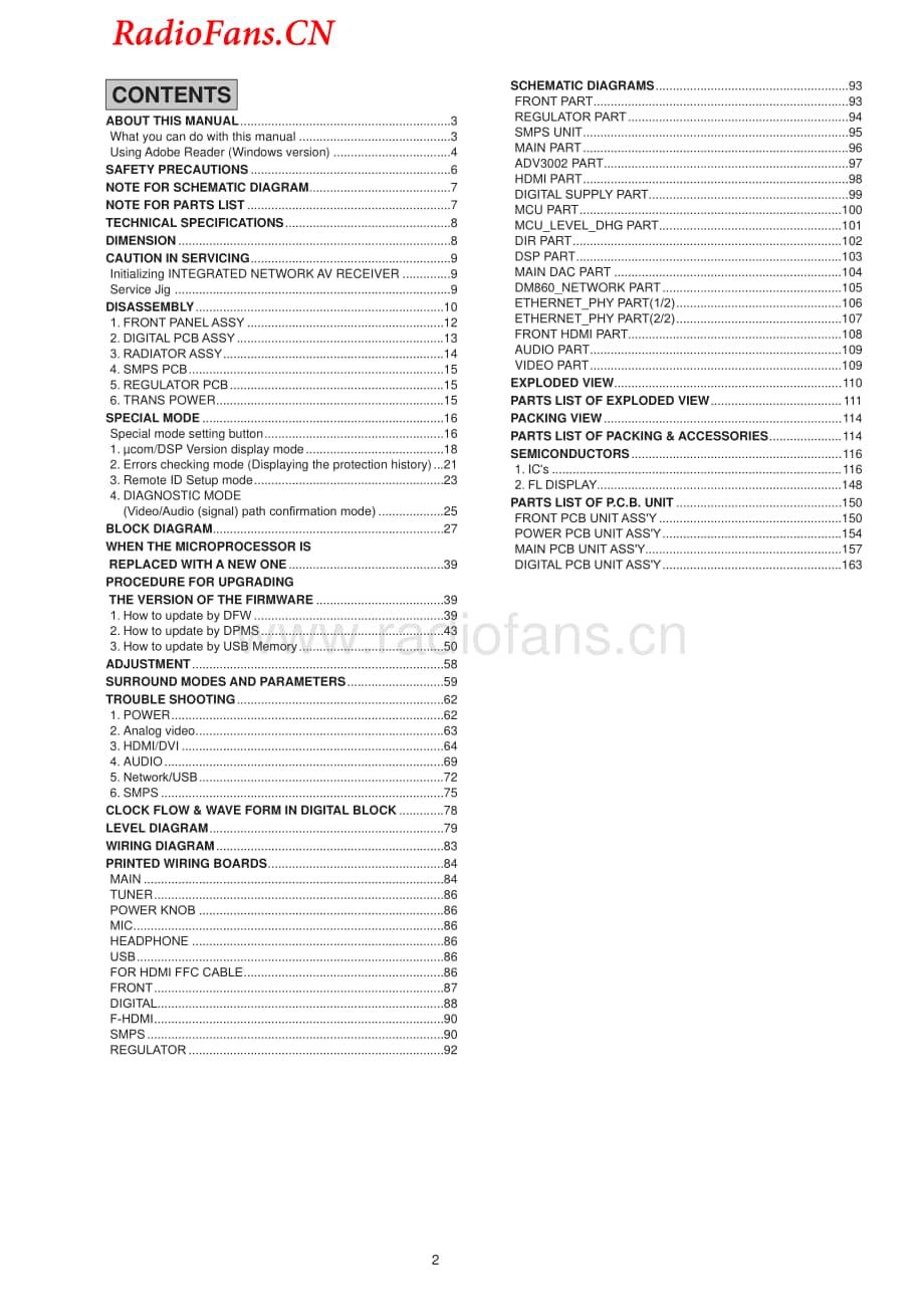
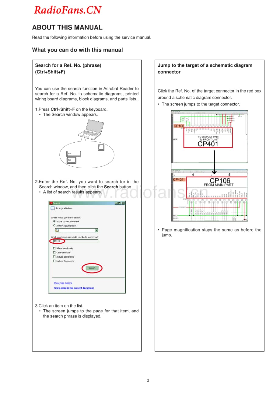
《Denon-AVR1613-avr-sm维修电路图 手册.pdf》由会员分享,可在线阅读,更多相关《Denon-AVR1613-avr-sm维修电路图 手册.pdf(186页珍藏版)》请在收音机爱好者资料库上搜索。
1、D supports TMDS logic level. 48 TXC+ HDMI output Diferential Clock Output. Diferential clock output at the TMDS clock rate; supports TMDS logic level. 49 TXGND Ground TXAVDD Ground. 50 TX0 HDMI output Diferential Output Channel 0 Complement. Diferential output of the red data at 10 the pixel clock r
2、ate; supports TMDS logic level. 51 TX0+ HDMI output Diferential Output Channel 0 True. Diferential output of the red data at 10 the pixel clock rate; supports TMDS logic level. 52 TXGND Ground TXAVDD Ground. 53 TX1 HDMI output Diferential Output Channel 1 Complement. Diferential output of the red da
3、ta at 10 the pixel clock rate; supports TMDS logic level. 54 TX1+ HDMI output Diferential Output Channel 1 True. Diferential output of the red data at 10 the pixel clock rate; supports TMDS logic level. 55 TXAVDD Power 1.8 V Power Supply for TMDS Outputs. RadioFans.CN 119 Pin No. Mnemonic Type Descr
4、iption 13 RXC_2 HDMI input Digital Input Channel 2 Complement of Port C in the HDMI Interface. 14 RXC_2+ HDMI input Digital Input Channel 2 True of Port C in the HDMI Interface. 15 HP_CTRLD Digital output Hot Plug Detect for Port D. 16 5V_DETD Digital input 5 V Detect Pin for Port D in the HDMI Inte
5、rface. 17 DGND Ground DVDD Ground. 18 DVDD Power Digital Supply Voltage (1.8 V). 19 DDCD_SDA Digital I/O HDCP Slave Serial Data Port D. DDCD_SDA is a 3.3 V input/output that is 5 V tolerant. 20 DDCD_SCL Digital input HDCP Slave Serial Clock Port D. DDCD_SCL is a 3.3 V input that is 5 V tolerant. 21
6、CVDD Power Receiver Comparator Supply Voltage (1.8 V). 22 CGND Ground TVDD and CVDD Ground. 23 RXD_C HDMI input Digital Input Clock Complement of Port D in the HDMI Interface. 24 RXD_C+ HDMI input Digital Input Clock True of Port D in the HDMI Interface. 25 TVDD Power Receiver Terminator Supply Volt
7、age (3.3 V). 26 RXD_0 HDMI input Digital Input Channel 0 Complement of Port D in the HDMI Interface. 27 RXD_0+ HDMI input Digital Input Channel 0 True of Port D in the HDMI Interface. 28 CGND Ground TVDD and CVDD Ground. 29 RXD_1 HDMI input Digital Input Channel 1 Complement of Port D in the HDMI In
8、terface. 30 RXD_1+ HDMI input Digital Input Channel 1 True of Port D in the HDMI Interface. 31 TVDD Power Receiver Terminator Supply Voltage (3.3 V). 32 RXD_2 HDMI input Digital Input Channel 2 Complement of Port D in the HDMI Interface. 33 RXD_2+ HDMI input Digital Input Channel 2 True of Port D in
9、 the HDMI Interface. 34 CVDD Power Receiver Comparator Supply Voltage (1.8 V). 35 CGND Ground TVDD and CVDD Ground. 36 TXPVDD Power 1.8 V Power Supply for Digital and I/O Power Supply. This pin supplies power to the digital logic and I/Os. It should be fltered and as quiet as possible. 37 TXPLVDD Po
10、wer 1.8 V Power Supply. 38 TXGND Ground TXPVDD Ground. 39 TXPGND Ground TXPLVDD Ground. 40 EXT_SWING Analog input This pin sets the internal reference currents. Place an 887 resistor (1% tolerance) between this pin and ground. 41 HPD_ARC Analog input Hot Plug Detect Signal. This pin indicates to the
11、 interface whether the receiver is connected. It supports 1.8 V to 5 V CMOS logic levels. 42 ARC+ Analog input Audio Return Channel Input (5 V Tolerant). 43 TXDDC_SDA Digital I/O Serial Port Data I/O to Receiver. This pin serves as the master to the DDC bus. It supports a 5 V CMOS logic level. 44 TX
12、DDC_SCL Digital output Serial Port Data Clock to Receiver. This pin serves as the master clock for the DDC bus. It supports a 5 V CMOS logic level. 45 TXAVDD Power 1.8 V Power Supply for TMDS Outputs. 46 TXGND Ground TXAVDD Ground. 47 TXC HDMI output Diferential Clock Output. Diferential clock outpu
13、t at the TMDS clock rate; supports TMDS logic level. 48 TXC+ HDMI output Diferential Clock Output. Diferential clock output at the TMDS clock rate; supports TMDS logic level. 49 TXGND Ground TXAVDD Ground. 50 TX0 HDMI output Diferential Output Channel 0 Complement. Diferential output of the red data
14、 at 10 the pixel clock rate; supports TMDS logic level. 51 TX0+ HDMI output Diferential Output Channel 0 True. Diferential output of the red data at 10 the pixel clock rate; supports TMDS logic level. 52 TXGND Ground TXAVDD Ground. 53 TX1 HDMI output Diferential Output Channel 1 Complement. Diferent
15、ial output of the red data at 10 the pixel clock rate; supports TMDS logic level. 54 TX1+ HDMI output Diferential Output Channel 1 True. Diferential output of the red data at 10 the pixel clock rate; supports TMDS logic level. 55 TXAVDD Power 1.8 V Power Supply for TMDS Outputs. RadioFans.CN 120 Pin
16、 No. Mnemonic Type Description 99 PGND Ground PVDD Ground. 100 PVDD Power PLL Supply Voltage (1.8 V). 101 XTAL Miscellaneous analog Input pin for 28.63636 MHz crystal or an external 1.8 V 28.63636 MHz clock oscillator source to clock the ADV7623. 102 XTAL1 Miscellaneous analog Crystal Output Pin. Th
17、is pin should be left foating if a clock oscillator is used. 103 PVDD Power PLL Supply Voltage (1.8 V). 104 PGND Ground PVDD Ground. 105 HP_CTRLA Digital output Hot Plug Detect for Port A. 106 5V_DETA Digital input 5 V Detect Pin for Port A in the HDMI Interface. 107 RTERM Miscellaneous analog This
18、pin sets the internal termination resistance. A 500 resistor between this pin and ground should be used. 108 DDCA_SDA Digital I/O HDCP Slave Serial Data Port A. DDCA_SDA is a 3.3 V input/output that is 5 V tolerant. 109 DDCA_SCL Digital input HDCP Slave Serial Clock Port A. DDCA_SCL is a 3.3 V input
19、 that is 5 V tolerant. 110 CVDD Power Receiver Comparator Supply Voltage (1.8 V). 111 CGND Ground TVDD and CVDD Ground. 112 RXA_C HDMI input Digital Input Clock Complement of Port A in the HDMI Interface. 113 RXA_C+ HDMI input Digital Input Clock True of Port A in the HDMI Interface. 114 TVDD Power
20、Receiver Terminator Supply Voltage (3.3 V). 115 RXA_0 HDMI input Digital Input Channel 0 Complement of Port A in the HDMI Interface. 116 RXA_0+ HDMI input Digital Input Channel 0 True of Port A in the HDMI Interface. 117 CGND Ground TVDD and CVDD Ground. 118 RXA_1 HDMI input Digital Input Channel 1
21、Complement of Port A in the HDMI Interface. 119 RXA_1+ HDMI input Digital Input Channel 1 True of Port A in the HDMI Interface. 120 TVDD Power Receiver Terminator Supply Voltage (3.3 V). 121 RXA_2 HDMI input Digital Input Channel 2 Complement of Port A in the HDMI Interface. 122 RXA_2+ HDMI input Di
22、gital Input Channel 2 True of Port A in the HDMI Interface. 123 HP_CTRLB Digital output Hot Plug Detect for Port B. 124 5V_DETB Digital input 5 V Detect Pin for Port B in the HDMI Interface. 125 DGND Ground DVDD Ground. 126 DVDD Power Digital Supply Voltage (1.8 V). 127 DDCB_SDA Digital I/O HDCP Sla
23、ve Serial Data Port B. DDCB_SDA is a 3.3 V input/output that is 5 V tolerant. 128 DDCB_SCL Digital input HDCP Slave Serial Clock Port B. DDCB_SCL is a 3.3 V input that is 5 V tolerant. 129 CVDD Power Receiver Comparator Supply Voltage (1.8 V). 130 CGND Ground TVDD and CVDD Ground. 131 RXB_C HDMI inp
24、ut Digital Input Clock Complement of Port B in the HDMI Interface. 132 RXB_C+ HDMI input Digital Input Clock True of Port B in the HDMI Interface. 133 TVDD Power Receiver Terminator Supply Voltage (3.3 V). 134 RXB_0 HDMI input Digital Input Channel 0 Complement of Port B in the HDMI Interface. 135 R


- 配套讲稿:
如PPT文件的首页显示word图标,表示该PPT已包含配套word讲稿。双击word图标可打开word文档。
- 特殊限制:
部分文档作品中含有的国旗、国徽等图片,仅作为作品整体效果示例展示,禁止商用。设计者仅对作品中独创性部分享有著作权。
- 关 键 词:
- Denon-AVR1613-avr-sm维修电路图 手册 Denon AVR1613 avr sm 维修 电路图
 收音机爱好者资料库所有资源均是用户自行上传分享,仅供网友学习交流,未经上传用户书面授权,请勿作他用。
 Denon-AVR1613-avr-sm维修电路图 手册.pdf


 Crown-XLS202-pwr-sch维修电路图 手册.pdf


